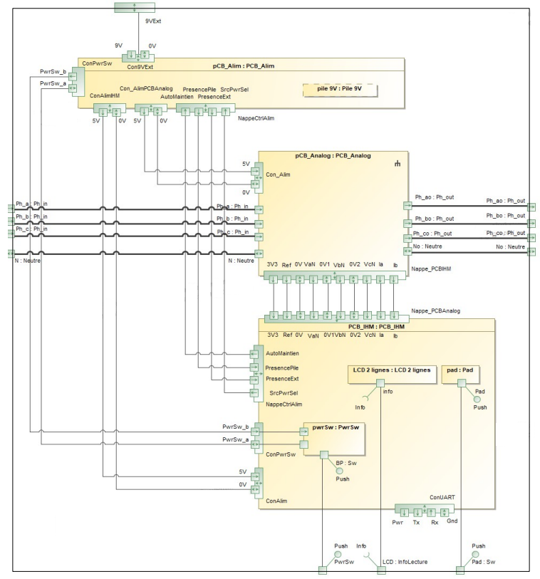
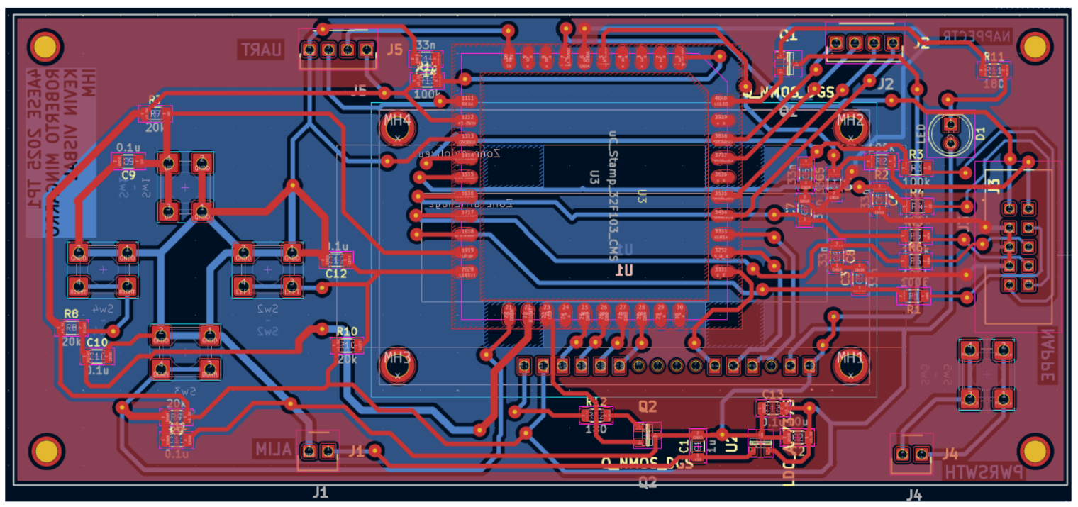
Digital Wattmeter PCB Design (STM32 + KiCad)

Engineering portfolio article · Schematic, PCB, fabrication, and bring-up evidence

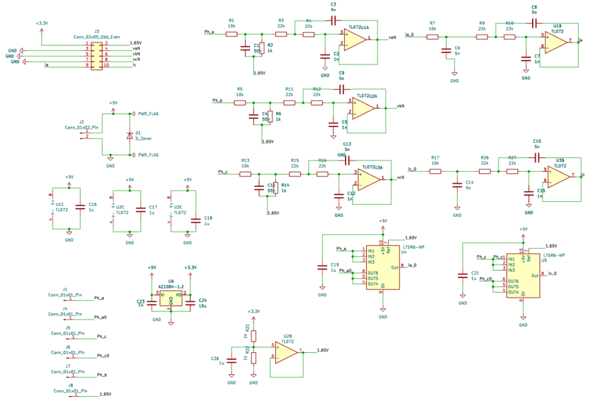
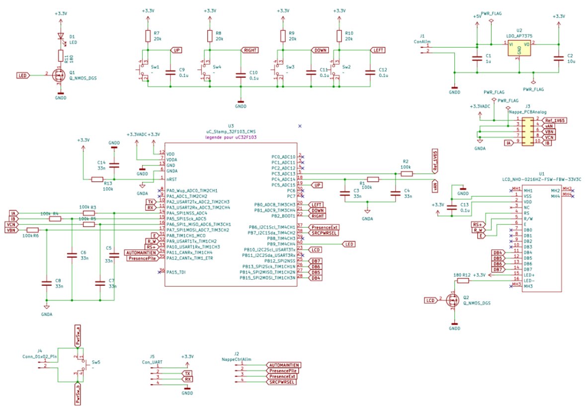
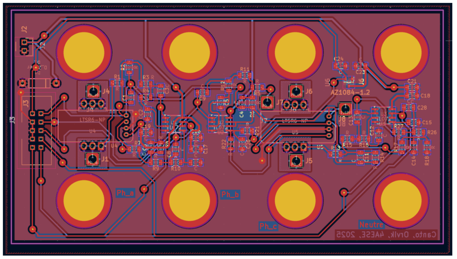
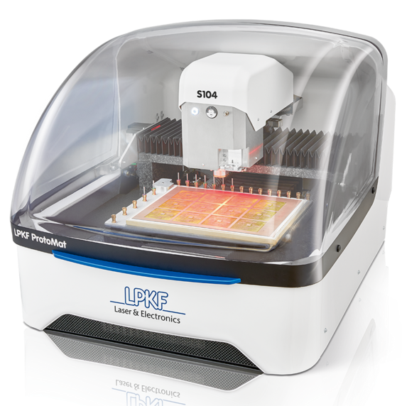
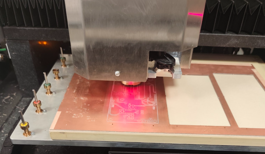
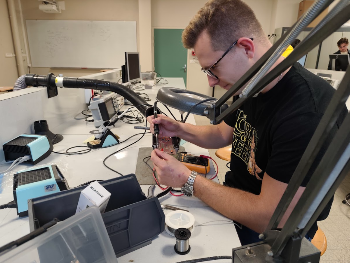
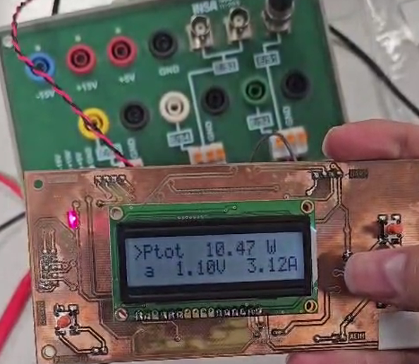
End-to-end engineering of a digital wattmeter platform spanning analog front-end design, STM32 integration, PCB layout and in-house fabrication. The implementation emphasizes manufacturable hardware decisions, clean measurement paths, and repeatable validation from assembly through functional bring-up.

  • STM32
  • KiCad
  • Analog front-end
  • PCB milling
  • Validation

System Architecture

  • Top-level partition of sensing, analog conditioning, MCU processing, and user-interface functions.
  • Defines signal flow and implementation constraints for the complete wattmeter platform.
Wattmeter architecture overview
Figure 1 — System architecture of the digital wattmeter platform.
Analog stage schematic
Figure 2 — Analog schematic including conditioning and measurement stages.

Analog Schematic

  • Acquisition path designed for robust measurement quality and noise-aware conditioning.
  • Component-level choices aligned with calibration and manufacturability targets.

HMI Schematic

  • User interface electronics and control logic integrated with the main embedded platform.
  • Design prioritizes readability, operational safety, and deterministic interaction.
HMI schematic
Figure 3 — Human-machine interface schematic.
Analog board layout
Figure 4 — Analog PCB layout with routing and grounding strategy.

Analog PCB Layout

  • Placement/routing optimized for signal integrity and coupling control.
  • Clear separation between sensitive analog areas and digital activity.

HMI PCB Layout

  • UI-focused layout balancing connector accessibility and board compactness.
  • Supports reliable assembly and serviceability.
HMI board layout
Figure 5 — HMI PCB layout implementation.
LPKF prototyping machine
Figure 6 — PCB prototyping setup using LPKF equipment.

Fabrication Setup

  • Rapid prototyping workflow configured for repeatable board production.
  • Process control centered on dimensional consistency and turnaround speed.

Isolation Milling

  • Isolation milling strategy used to realize traces and clearances in-house.
  • Toolpath and machining parameters tuned to reduce defects.
Isolation milling process
Figure 7 — Isolation milling operation during PCB manufacturing.
Fabricated boards
Figure 8 — Fabricated bare boards after machining and inspection.

Fabricated Boards

  • Post-process inspection verifies continuity, isolation, and dimensional tolerance.
  • Boards prepared for assembly and staged validation.

Assembly

  • Controlled soldering sequence applied to analog and UI assemblies.
  • Rework criteria and visual inspection checkpoints ensure build quality.
Board soldering stage
Figure 9 — Soldering and assembly phase.
Hardware bring-up test
Figure 10 — Hardware bring-up and initial validation tests.

Bring-up & Validation

  • Incremental power-up and functional verification from rails to full operation.
  • Measurement consistency checks and issue tracking close the hardware loop.

Deliverables

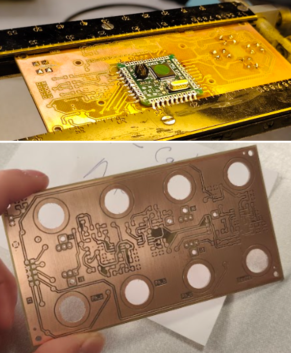
This page captures the engineering narrative. The full PDF includes complete implementation details, validation evidence, and final manufacturing documentation.